Direct manufacturer-grade interface components engineered for reliability, safety compliance, and robust data integration across diversified industrial deployments.
In a global landscape saturated with narratives around USB4, Thunderbolt 4, and multi-gigabit throughput protocols, a critical reality remains evident to embedded systems engineers and procurement officers: USB 2.0 remains a foundational pillar of modern industrial, commercial, and consumer infrastructure. The global demand for USB 2.0 interconnect systems, adapters, and physical transceiver layers has not diminished; rather, it has transitioned into a highly mature, specialized, and cost-sensitive market segment.
From a product life-cycle perspective, USB 2.0 (specifically the USB 2.0 High-Speed specification operating at 480 Mbps) provides the absolute optimal ratio of silicon footprint, licensing overhead, power efficiency, and signal transmission line distance. High-speed transceivers running USB 3.0 (5 Gbps) and beyond require complex equalizer circuits, low-jitter reference clocks, and significantly higher standby power consumption. For applications where telemetry data, peripheral command structures, or audio signals are processed, paying the premium for high-bandwidth interfaces is commercially inefficient and technically unnecessary.
Furthermore, electromagnetic compatibility (EMC) is a primary consideration in critical operating environments. The higher fundamental frequency of USB 3.0 signals generates broadband radio frequency interference (RFI) that directly overlaps with the 2.4 GHz ISM band. This phenomenon is known to degrade the sensitivity of nearby Wi-Fi, Bluetooth, and ZigBee wireless receivers. In contrast, USB 2.0 operates at a much cleaner spectrum profile, allowing co-located microcontrollers and RF transmitters to function without expensive shielding enclosures. For this reason, medical equipment, industrial PLCs, and telecommunication switches consistently mandate USB 2.0 connectivity.
Procuring discount USB 2.0 cables or adapters does not mean accepting sub-standard electrical performance. The physical layer (PHY) layout requirements of the USB 2.0 specification are exacting. Differential signals D+ and D- must navigate a strict 90 Ω (ohm) differential impedance envelope. A divergence of even 10% in line impedance can cause massive signal reflections, resulting in high packet loss rates, packet re-transmissions, and ultimate connection drops.
To ensure high transmission integrity over run lengths up to 5 meters, Dongguan Taitron Electronics utilizes advanced physical manufacturing processes:
| Electrical Parameter | USB 2.0 Specifications | USB 3.0 / 3.1 Gen 1 Specifications | Industrial Sourcing Advantage |
|---|---|---|---|
| Nominal Data Rate | 480 Mbps (High-Speed) | 5 Gbps (SuperSpeed) | Highly adequate for control loops and diagnostic feeds. |
| Differential Impedance | 90 Ω ± 15% | 90 Ω ± 7% | Wider tolerances allow significantly lower manufacturing reject rates. |
| Max Recommended Length | 5.0 Meters (Passive) | 2.0 - 3.0 Meters (Passive) | Superior physical range without requiring expensive active repeaters. |
| 2.4 GHz Band RFI | Negligible | High (requires intensive shielding) | Eliminates RF design complications in IoT nodes and medical carts. |
| Unit Cost Index | Baseline (1.0x) | 3.5x - 5.0x | Maximum cost reduction for large-scale enterprise deployments. |
How modern industries deploy USB 2.0 physical interfaces to maintain operational continuity and cost-efficient hardware scaling.
On high-voltage factory floors, Programmable Logic Controllers (PLCs) and CNC mills use USB 2.0 interfaces for programming and diagnostic data transmission. The lower frequency of USB 2.0 avoids interference from adjacent high-frequency motor drives, while its high mechanical durability withstands temperature swings and physical vibration.
Medical imaging equipment, ultrasound probes, and patient monitor terminals rely heavily on customized USB 2.0 assemblies. Due to strict leakage current limitations imposed by IEC 60601-1 standards, USB 2.0’s simpler layout allows for integrated optical or magnetic galvanic isolation circuits to be implemented cost-effectively.
Vehicle electronic control units (ECUs) and diagnostic ports utilize USB 2.0 interfaces for flashing firmware and collecting engine logs. The resilience of the physical layer against massive temperature shifts (-40°C to +85°C) and custom locking connector housings ensure continuous data retention during automotive test sweeps.
Our organization’s trajectory exemplifies the evolution of advanced audio, video, and data transmission manufacturing over the past four decades. Originally founded in 1984 as Tonetron in Keelung, Taiwan, our founders realized early that global demand for precision cable systems would require vast production scalability and localized raw material efficiency. Consequently, in 1993, we moved our main operations to a self-built, independent production industrial park in Dalingshan Town, Dongguan City, China, officially changing our name to Dongguan Taitron Electronics Limited.
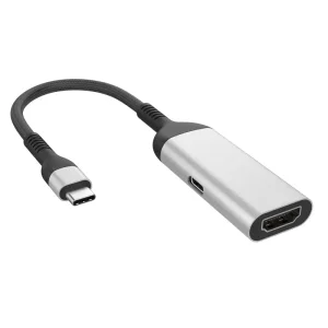
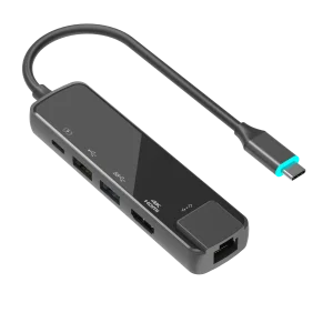
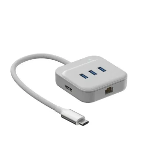
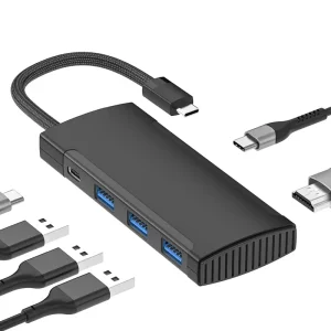
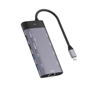
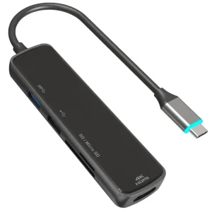
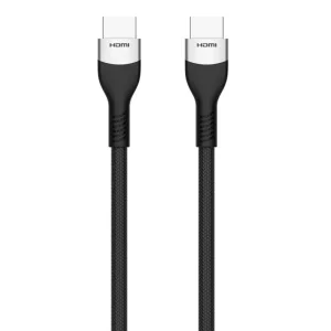
For more than 38 years, we have leveraged this independent manufacturing hub to master the development and production of high-end connection lines. While we offer highly cost-optimized discount USB 2.0 configurations, our facility simultaneously designs and builds ultra-high-speed interfaces such as HDMI 2.1 cables, DP 2.0 cables, USB4 data lines, USB-C 3.1 Gen2 components, and multi-functional Type-C expansion docks.
This cross-disciplinary engineering capability guarantees that even our standard legacy product lines benefit from the same high-tier quality management workflows, material selection, and rigorous environmental compliance testing that we apply to our high-frequency 8K/10K transmission systems.
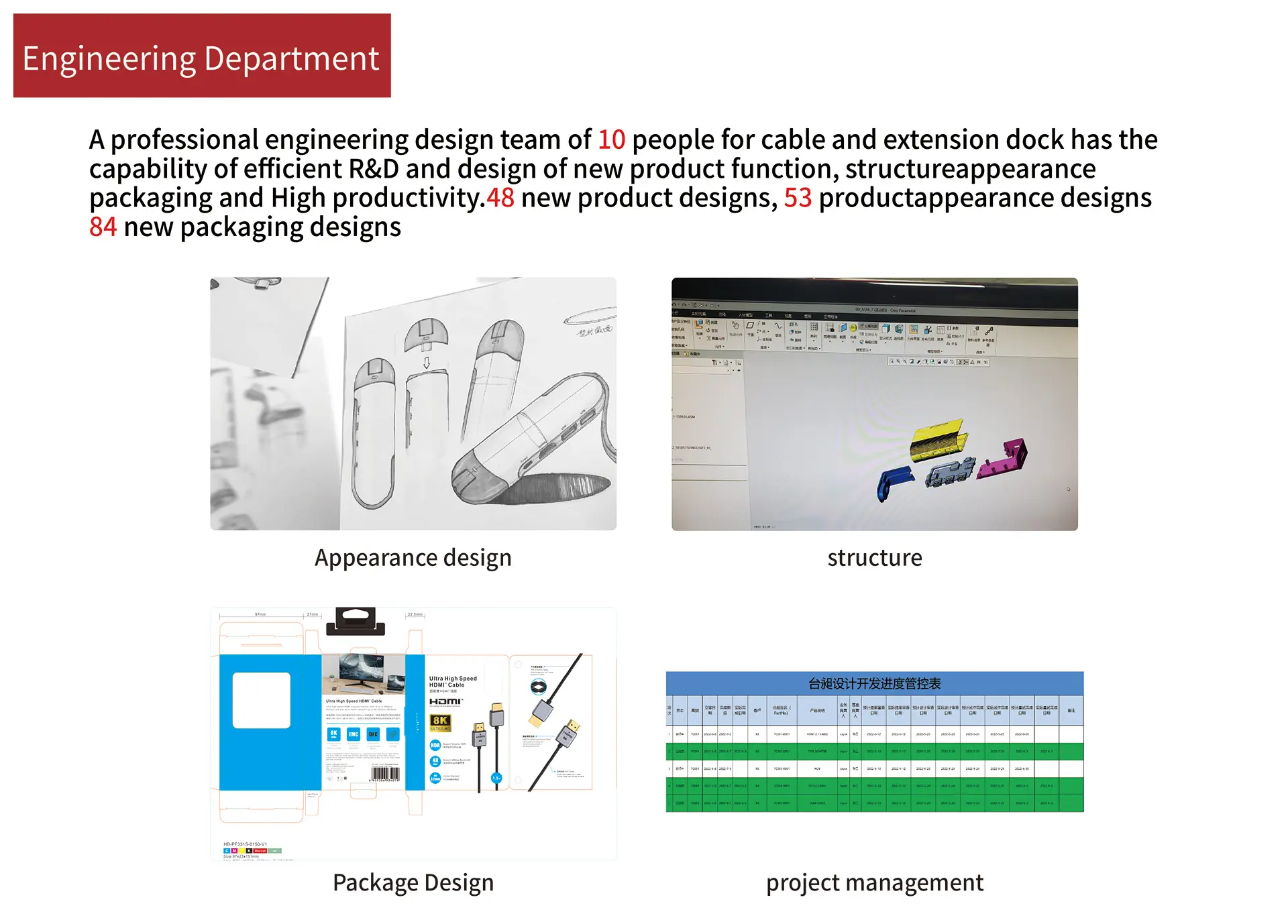

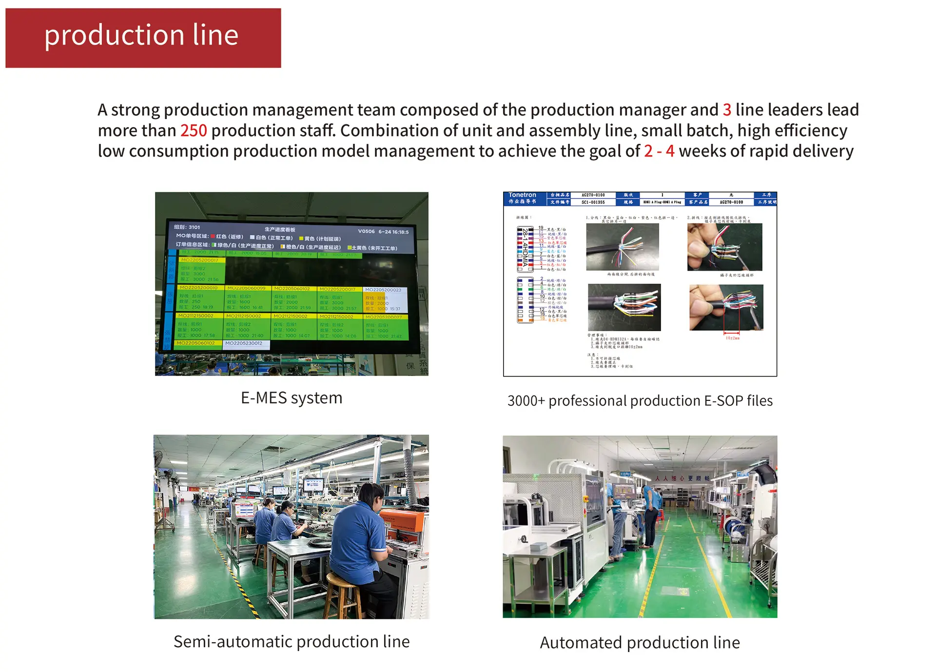
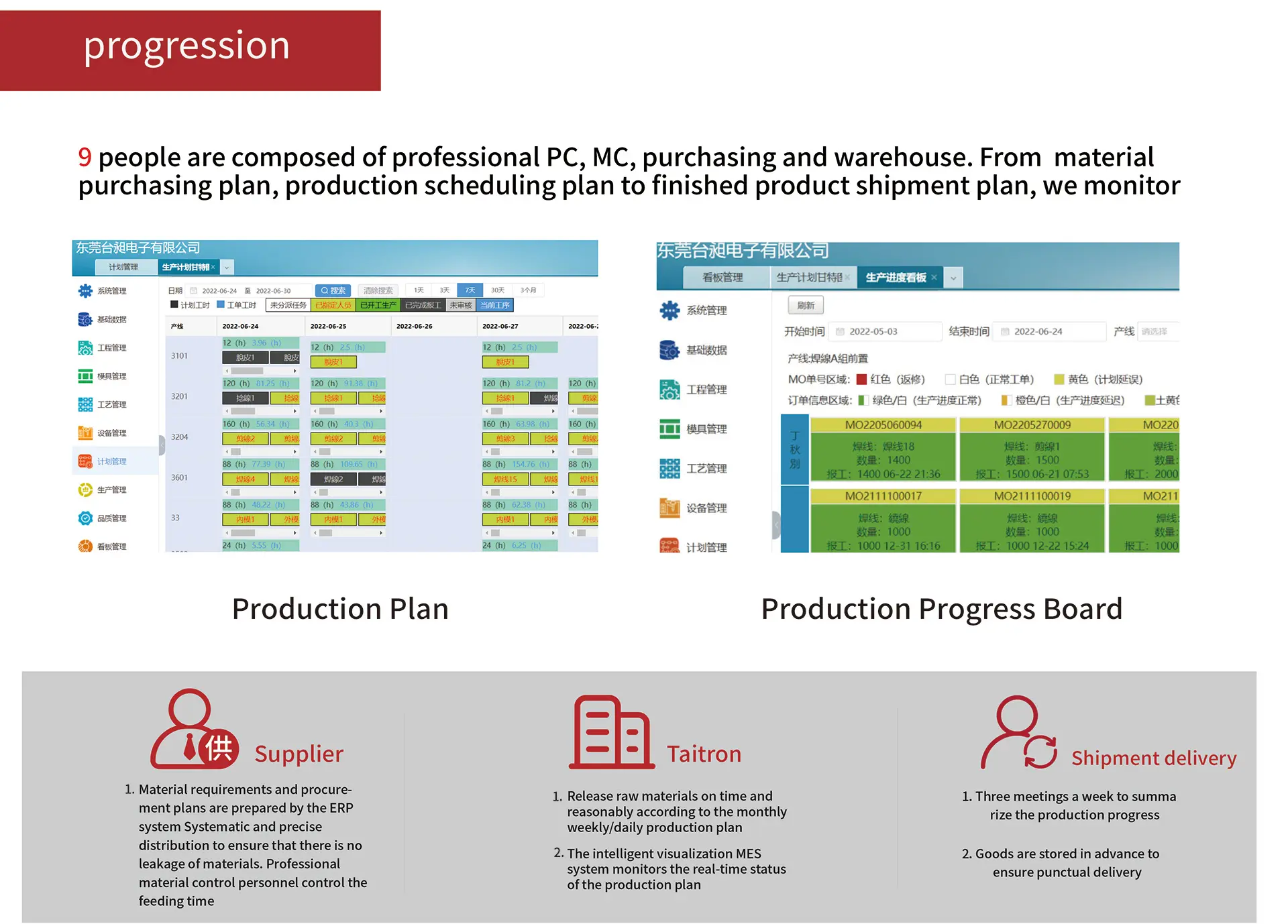
By keeping raw copper drawing, PVC compound formulation, terminal gold-plating, wire extrusion, and dual-shot overmolding inside our own Dalingshan industrial park, we maintain total control over our production schedule and quality checks. This integrated approach shields our global buyers from typical supply chain blockages and guarantees stable price tiers even during market volatility.
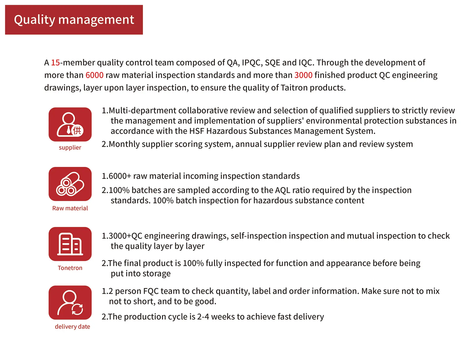
Every cable batch is tested using high-performance electronic network analyzers and time-domain reflectometers (TDR) to confirm impedance values. Mechanical endurance is verified via automatic bending testers (simulating 10,000+ flex cycles), salt spray chambers for corrosion protection, and strict terminal extraction force meters.
For B2B procurement managers sourcing parts for Europe, North America, and parts of Asia, simple compliance claims are not enough. High-volume purchases must align with strict international directives to avoid costly import delays, customs hold-ups, or consumer-safety recalls. Our entire product line, from entry-level legacy cables to complex multi-port docking systems, is built to clear these international regulatory hurdles:
RoHS & REACH Directives: We verify that all insulation jackets, inner shields, solder junctions, and plastic housings are free of restricted hazardous compounds (such as lead, cadmium, mercury, and polybrominated biphenyls). This ensures our products are fully compliant with European Union environmental standards.
CE and FCC Certifications: Electromagnetic compatibility is verified through designated testing laboratories. This certifies that our shielded cable lines and adapters do not emit unwanted RF signals and possess high resistance to ESD (electrostatic discharge) events typical of dry, climate-controlled office spaces or heavy factory floors.
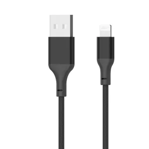
MFi Certification Experience: As a seasoned manufacturer of premium components, we maintain strict adherence to Apple's MFi manufacturing standards, which is evident in products like the MFi USB-A to Lightning interface (PLT347). This level of technical oversight is carried over into our generic USB 2.0 products, ensuring consistent plug-and-play reliability.
Find quick technical answers and procurement solutions for bulk USB 2.0 connectivity and customization projects.
USB 2.0 operates at a much lower signal frequency (240 MHz fundamental frequency for 480 Mbps data rates) compared to USB 3.0 (which generates broadband noise overlapping the 2.4 GHz spectrum). This lower frequency profile reduces electromagnetic interference (EMI) risks around industrial equipment and nearby wireless devices. Additionally, USB 2.0 components are much less sensitive to slight connector wear, are cheaper to produce, and support longer passive cable lengths (up to 5 meters) without signal boosters.
We maintain a target differential impedance of 90 Ω ± 15% across our production lines. This is achieved by using automated extrusion machinery that precisely controls the dielectric spacing between the D+ and D- twisted pairs. We verify these settings using Time-Domain Reflectometry (TDR) testing during both production runs and final quality control audits.
Yes, we provide full ODM services, including custom tool design and injection molding inside our Dongguan Dalingshan industrial park. We can adjust the flexibility of the strain relief using PVC, TPU, or other thermoplastic elastomers to match the specific wear patterns and vibration levels of your application.
We conduct regular material audits using X-ray fluorescence (XRF) screening during material intake. For final product batches, we utilize accredited third-party labs to perform Inductively Coupled Plasma Optical Emission Spectrometry (ICP-OES) analysis, ensuring that lead, phthalates, and other restricted chemicals remain well below regulatory limits.
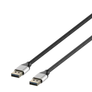
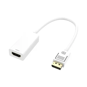
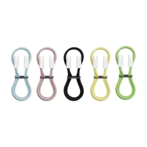
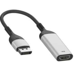
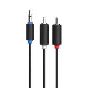
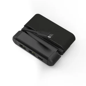
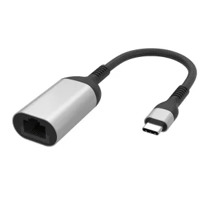
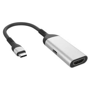
Additional interface components, high-speed converter assemblies, and audio/video connection lines manufactured under our strict ISO quality framework.
 Taichang Electronic